Tips for PCB Design
To avoid listing pcb parameters but still specify them for RFQs, POs, etc., we are introducing standard types. The basic standard type is the most commonly ordered pcb type: 2 layer, min 1 oz copper, pth, 1.6 mm thick, FR4, solder mask green x2, silk screen white x1, Enig finish, min trace and gap 5 mil, IPC Class 2,..
You are welcome to specify Std, Std_4L, or Std_6L_0.8mm etc. and list only non-standard parameters. Example: Std with 2.4 mm FR4 Tg135 and silk screen 2 sides, solder mask blue.
Otherwise necessary information to quote:
- Copper thickness Inner and outer layers
- Total thickness and required tolerance
- ML-build minimum isolation between layers
- Materials types, thicknesses
- Drill dimension table Number of holes and dimensions – in gerbers
- Complete drawing Gerber outline and tolerances.
- solder surface finish Solder surface
- Type of solder mask Color, 1 or 2 side
- Type of legend print Color, 1 or 2 side
- Net list IPC 356 are preferred
Check list for Designer
- Plated/unplated hole in different files, drill files or gerber files
- Name and mark layers in order 1 to…max layer. Add text on outer layers to avoid mirroring!
- Add opening in solder mask for unplated holes
- Are vias not open in solder mask to be filled with solder mask only or also via fill ?
- Unused traces removed from design else advise about guard traces
- Is clearance around plated and unplated holes in inner layers correct?
Factors affecting costs
- Number of boards Factor is total batch area
- Delivery time Standard 15 works days, less for 1-5 smaller boards
- Board Size Complex larger pcbs higher unit area price than smaller
- Materials FR4 Tg130 is lowest cost for pth
- Class II or III Increased cost tracks and gaps less than 0,15mm (6 mil)
- Number of layers Increased cost
- Thickness Drill stack lower, laminate and freight costs up
- Number of holes The more the higher
- Hole less than 0,5mm Increased cost
- Number of test point Increases cost
- Type of surface finishes Tin/copper, Ni/Au, OSP, Silver………
- Blind or buried via layers Increased cost
- Micro-via layers May increase or decrease total cost
- Carbon print, peelable mask Increased cost
- Edge plating Increased cost
Optimized use of material
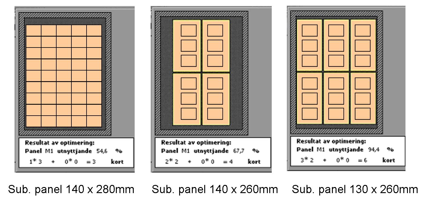
Another very important factor to consider in terms of economy and environment is how we use the surface of the panel for individual pcb layout.
This can have a significant effect on the price. The more cards we can get out of each panel, the better economies and it is also very important for the environment to have as little waste as possible.
In this example below the number of cards from same production panel varies from 12 to 45 pieces!
Panels routed and scored with panel bars typically 7-12 mm wide on two sides usually provide good yield with no assembly problems.
Ask us, we suggest panel layouts to customers every day !
Abbreviations
AOI Automatic Optic Inspection
BGA Ball Grid Array
BT Bismaleimide Trazine (BT-Epoxy)
CAD Computer Aided Design
CAF Conductive Anodic Filament
CAM Computer Aided Manufacturing
CSP Chip Scale Packing
CTE Coefficient of Thermal Expansion
Df Dissipation factor
Dk Dielectric constant
DRC Design Rule Check
ENIG Electroless Nickel Immersion Gold
ENIPIG Electroless Nickel Palladium Immersion Gold
FR 4 Flame Resistant 4
HASL Hot Air Solder Leveling
HASL Pb Free Hot Air Solder Leveling Lead Free
HDI High Density Interconnect
I/O Input/Output
IPC International Printed Circuit Association Connecting Electronics Industries (PCB/PCBA standards)
IR Infra Red
NPTH Non Plated Through Hole
MCM Multi Chip Module
OSP Organic Solderbility Preservaties
PCB Printed Circuit Board
PWB Printed Wiring Board
PTH Plated Through Hole
PTFE Polytetrafluorethylene (Teflon)
QFP Quad Flat Pack
RCC Resin Coated Copper
RoHS Restriction of Hazardous Substances
SMOBC Solder Mask Over Bare Copper
SMD Surface Mount Device
SMT Surface Mount Technology
Tg Glass transition temperature – when epoxy softens
UL Underwriter´s Laboratories
UV Ultra Violet